General Instructions
Special thanks to Paul Schreiber of Synthesis Technology, from whom these general recommendations have been adapted.
Tools
The most important factor in successful QBone kit building is having the proper tools. This does not mean the most expensive tools, but the correct tools. Having moderately proced tools will greatly speed the building process, and treated nicely, will last many years. The following is a list, in order of importance, of the tools you will need.
Soldering iron. The proper wattage is 35-70W. We recommend the Weller WE1010, which costs about US$110.
A good pair of diagonal or flush cutters. These cost about US$20.
A good pair of chain nose, serrated-jaws pliers. These also cost about US$20.
An anti-static wrist strap. This needs to be grounded to a power outlet. These vary in price from $5 for a disposable, one-time device to $50 for a nice watch-band style.
An awl or double-sided soldering aid. We recommend the Weller WLACCSAK-02, which costs about US$10.
An IC pin straightener. This is a spring-loaded plastic tool, which costs about US$7.50.
Soldering
Soldering is what kit-building is all about. It can be relaxing, like needlepoint, or very messy and frustrating. The difference is having the correct soldering iron, and practice. It is also a good idea to take a 5 minute break every 20 minutes or so.
Soldering is a high temperature adventure: the common soldering irons use 700F tips. Molten solder does cool extremely quickly, except when you get some on your skin.
The first rule of soldering is: use only enough to get the job done. Most soldering problems arise by using too much solder. It is easy to get carried away and glob a huge blob of solder on the connection.
The second rule is: heat the connection for about half a second before you apply solder. This pre-heating is used to prevent the molten solder from hitting cold metal and cooling too fast. This results in what’s called a cold joint, which is a loose connection where the solder did not adhere to the metal. The technique (which becomes automatic after a while) is to put the tip on the board first, and then apply the solder. Once the solder is on the joint, you hold the iron there for another half second, and pull the iron away. If the solder doesn’t flow easily, perhaps you haven’t allowed your iron to warm up, you have set the wrong temperature, or it is underpowered.
When you insert a part into the PC board (on the side of the board with the QBone lettering), the leads will need to be bent outwards before soldering. This is called a ‘cinch’. Also, it is important that the parts be all the way down on the PC board. Sockets will be slightly off the board, to allow the flux to be washed off (see below).
Remember, it's easy to add solder, but difficult to remove.
Solder & Flux
Our recommended assembly solder is Kester 24-7068-6403 (RoHS) or 24-6337-6403 (traditional, with lead). In order for solder to ‘stick’ to the joints, a chemical called ‘flux’ is inside the solder. This solder has 'organic flux': all you need to remove the flux residue is warm water. The residue is OSHA approved for washing down your drain safely.
After you solder about 20 parts on the PC board, you wash the board in a sink under warm water (50-60°C, or 120-140°F). Use a soft scrub brush, and scrub the solder joints thoroughly. A small scrub brush is best, but a toothbrush can do in a pinch. You may see the joints suds up, and if so, keep scrubbing for a little while after the sudsing stops. The water will not harm the parts on the PC board. Turn the board over and wash/scrub the top side as well. Do not use any soap or other cleanser!
The flux residue left on the board will cause high impedance paths between connections. This will make the board act funny. Also, over a long period of time (say, 6 months), the flux will cause corrosion of the metal parts. You don't want this!
After washing, blot it dry with a paper towel and let it air-dry for about 20 minutes. Then you can solder more parts. This is spelled out in the instructions: please follow this procedure.
You may be asking: why in the world are we going through all this trouble over solder? The answer is simple: no type of solder will give a high quality joint quite like organic solder will. When the board is washed and dried, the joints are near mirror finish. The older rosin-based fluxes leave a nasty brown reside which is very sticky and over the long run attracts moisture. This solder flux washes away 100% clean.
Parts List
Please check carefully that all of the parts are in your kit. If you suspect something is missing, email or call us. Be careful when opening the bags: some of these parts are very small!
-
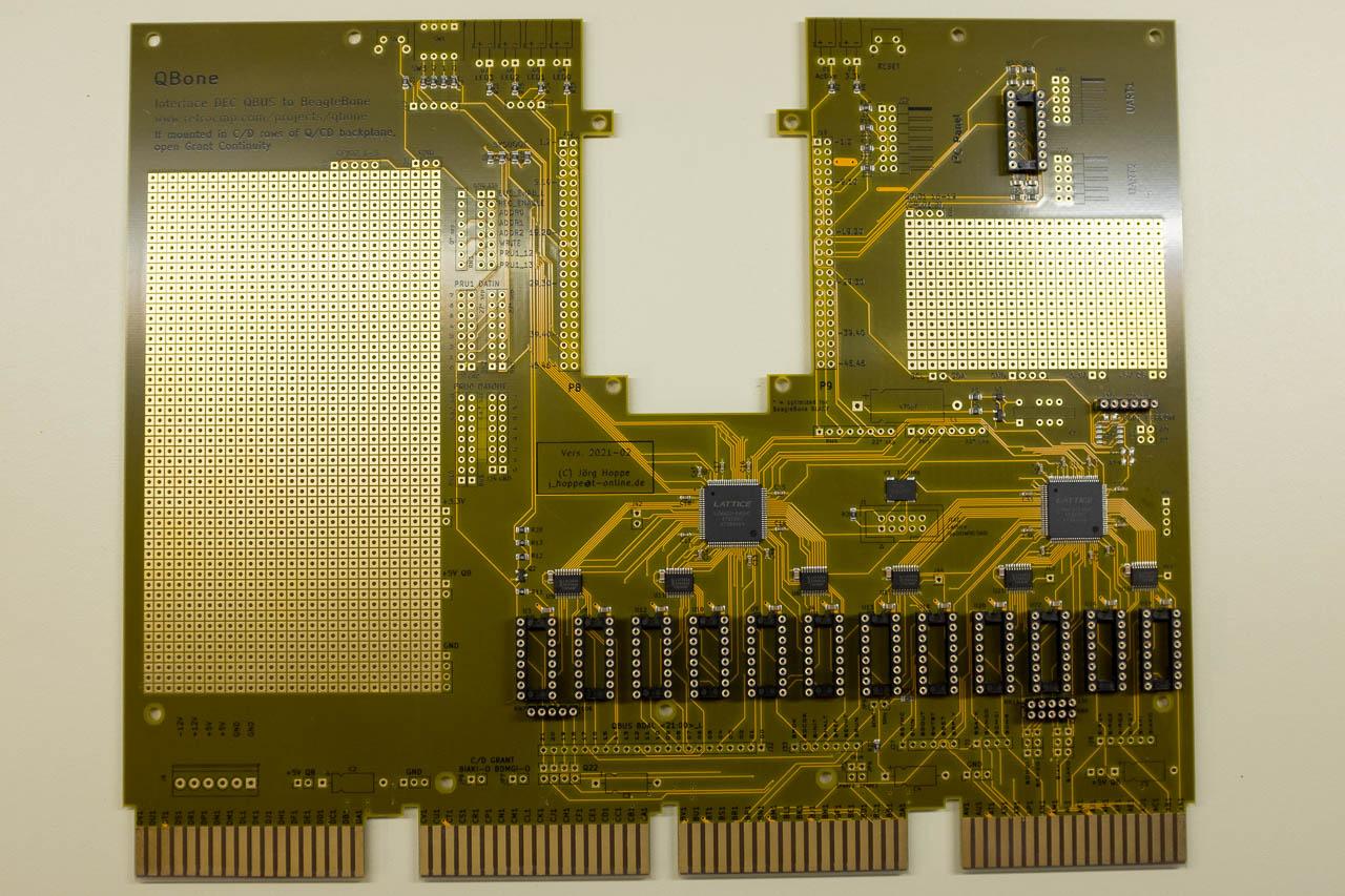
Circuit boards
1 QBone PCB with pre-riveted handles
2 Interposer PCBs (about the size of a stick of gum)
-
Switches and buttons
1 4-position “piano” style DIP switch
1 User button (long shaft)
1 Reset button (short shaft)
-
4 Resistor Arrays (tan, SIP form factor)
1 10kΩ bus array, SIP5
1 10kΩ bus array, SIP6
1 330Ω bus array, SIP5 or SIP6
1 680Ω bus array, SIP5
-
5 Capacitors
4 10μF 50V axial
1 470μF 16V axial
-
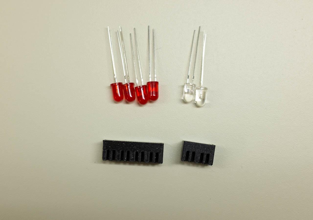
6 Light-Emitting Diodes (LEDs)
2 3mm Green LED
4 3mm Red LED
-
13 Integrated Circuits (ICs)
12 DS8641 drivers, DIP16
1 MAX3232, DIP16
-
Sockets, wires, & connectors
13 IC sockets, DIP16
20 2-pin insulated shunt wire (note: VERY small! Be careful!)
21-position milled SIP socket strip
2 2×23 pin header, gold plated, shifted
2 2×23 pin header, tinned, shifted
1 2×15 pin header, gold plated (4+3+3+2+1+1+1)
2 2×5 IDC connector, male, R/A
1 2×7 IDC connector, male, R/A
1 2x5 IDC connector, 2.54mm, female, R/A
1 DE-9 connector, male, free hanging, IDC
1 9pos grey flat ribbon cable, 28 AWG, 1m
1 Terminal block, 6 pos., 3.5mm
-
Other
1 BeagleBone Black
1 SDCard, 32GB, various mfrs., pre-loaded
1 2A 5VDC DPDT non-latch relay
13 shunt jumpers, various colours
1 4-position LED fixture, 3D printed
1 2-position LED fixture, 3D printed
1 3.5mm spacer, 3D printed
Part 0: Programming the CPLDs
If you opted for a kit without pre-programmed CPLDs, you will need to acquire a CPLD programmer capable of programming Lattice MachXO2 chips via JTAG.
Programming the CPLDs before populating the board is best. This way, your programmer can power only the CPLDs with its 3V3 line directly, without having to power the entire QBone from a bench supply.
Wiring is as follows:

If using the Lattice Diamond programming software, load the provided
qbone-machxo2-programmer.xcf file and press the Program button.
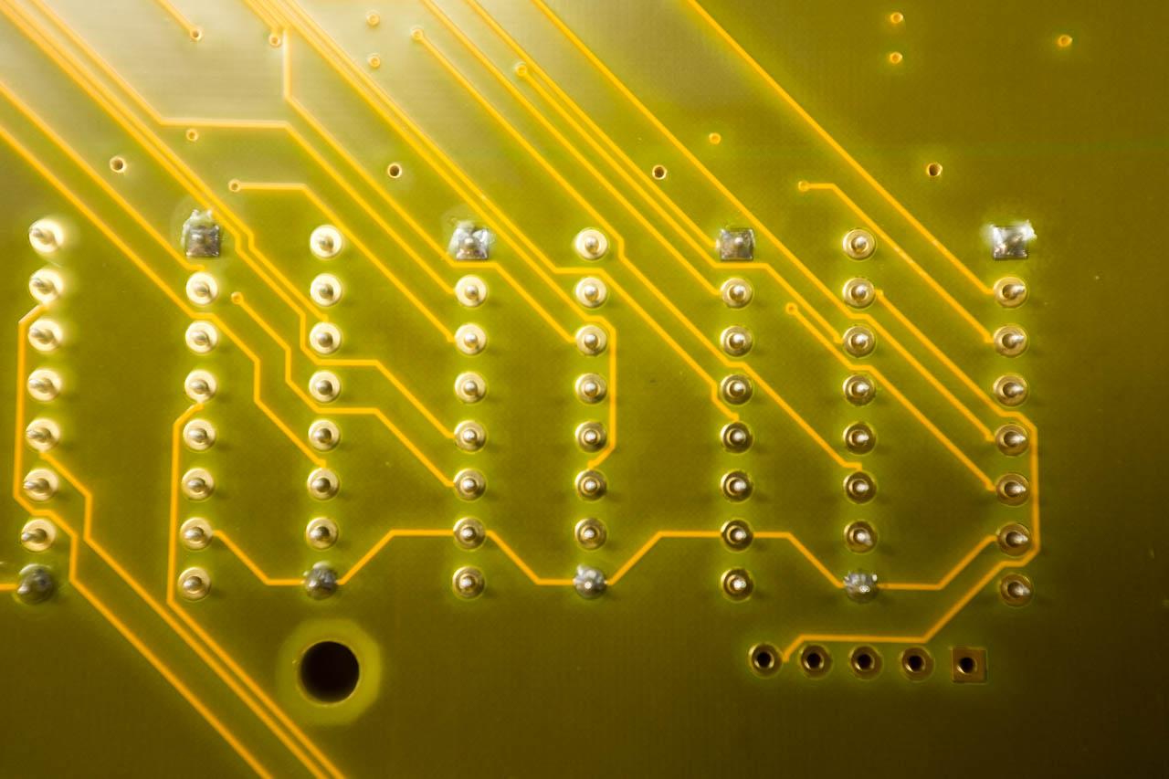
Part 1: Soldering the IC Sockets
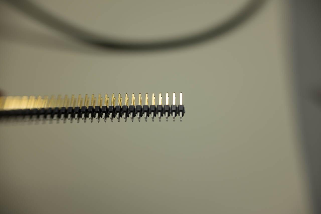
Since there are more IC pins than anything else, we will start here. For each IC socket:
Insert the socket with the notch facing up.
Hold the socket in place and flip the board over.
Solder two diagonally opposite corner pins, while holding the socket flush and your finger away from the hot pins. (If this worries you, hold the socket in place with a piece of painters' tape.)
Flip the board back over and ensure the socket is flat before continuing. If not, heat either or both of the corner pins and push the socket completely flat.
Solder the remaining pins to the PC Board.
Repeat this process for all 13 sockets.
Wash the board in warm water, gently scrubbing both sides. DO NOT USE ANY SOAP!
Shake the board a couple of times and blot dry with an old towel (the pins will fray a good towel). Let dry for at least 15 minutes.
Take a tea break! You are about 15% done.


Part 2: SIP sockets and wire links
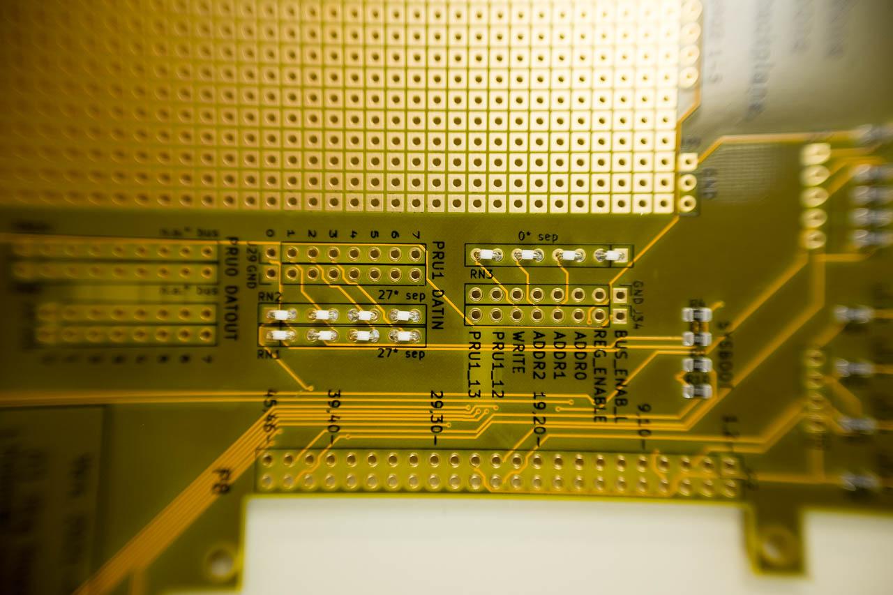
Using a pair of pliers, separate the SIP socket strip into 1 6-pin and 3 5-pin lengths. This is easiest if you hold the strip just past where you want to make the break, then press sideways with your fingers to snap the strip. If you have 2 pairs of pliers, grip on both sides and break in the middle.
Solder the 6-pin socket at RN6. Be sure the socket is seated flush against the board and is not pointed at an angle.
Solder the 5-pin sockets at RN7, RN11, and RN12.
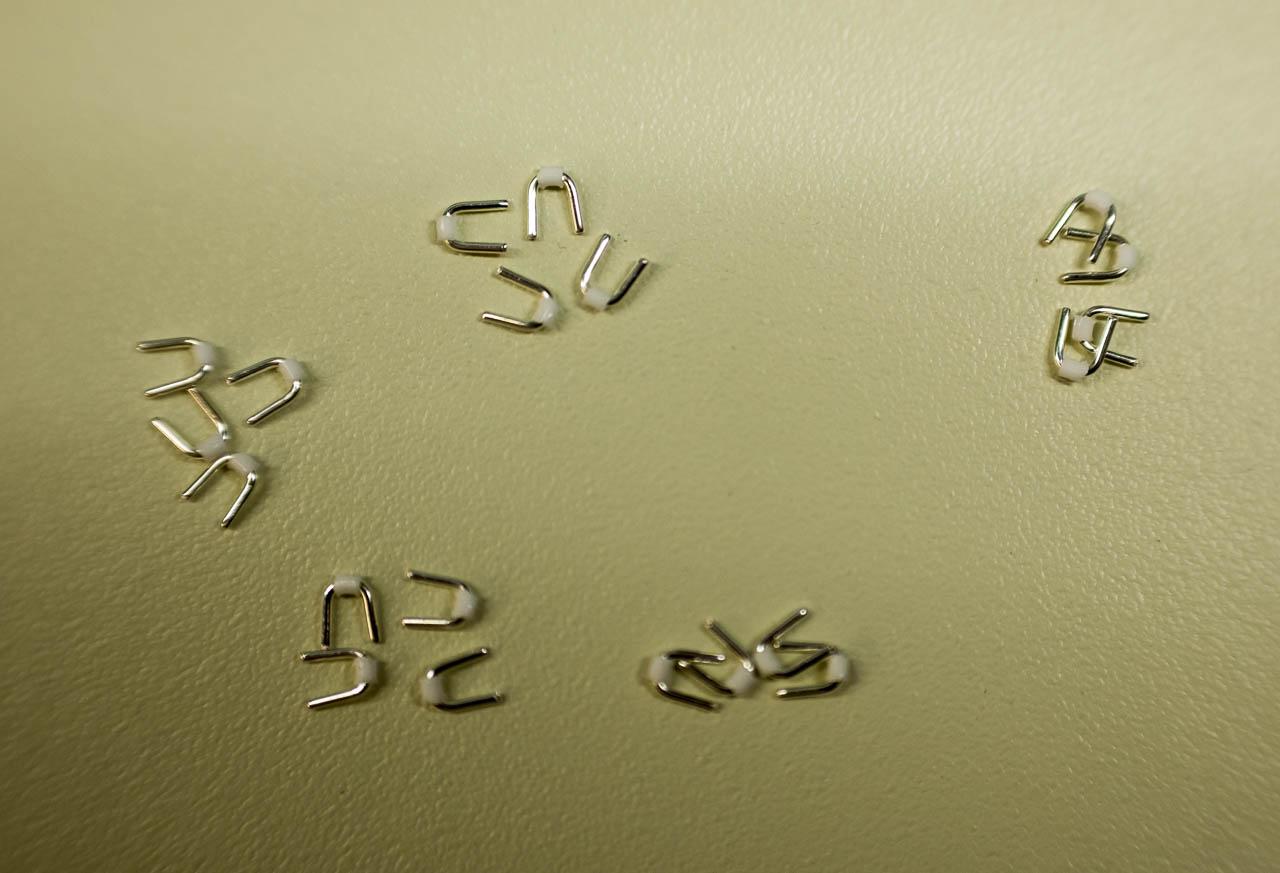
Find the 20 very small insulated wire links in the bottom of the bag. (If you lose any, you can replace them with short pieces of solid wire, or from discarded component leads.)
Insert wire links in adjacent pins for RN1, RN2, RN3, RN4, and RN5. Hold them in place with a piece of painter's or masking tape.
Solder the wire links in place, then remove the tape.
Wash the board again, gently scrubbing both sides where you have soldered. Use ONLY warm water!
Part 3: Capacitors and switches
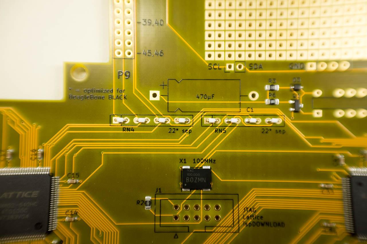
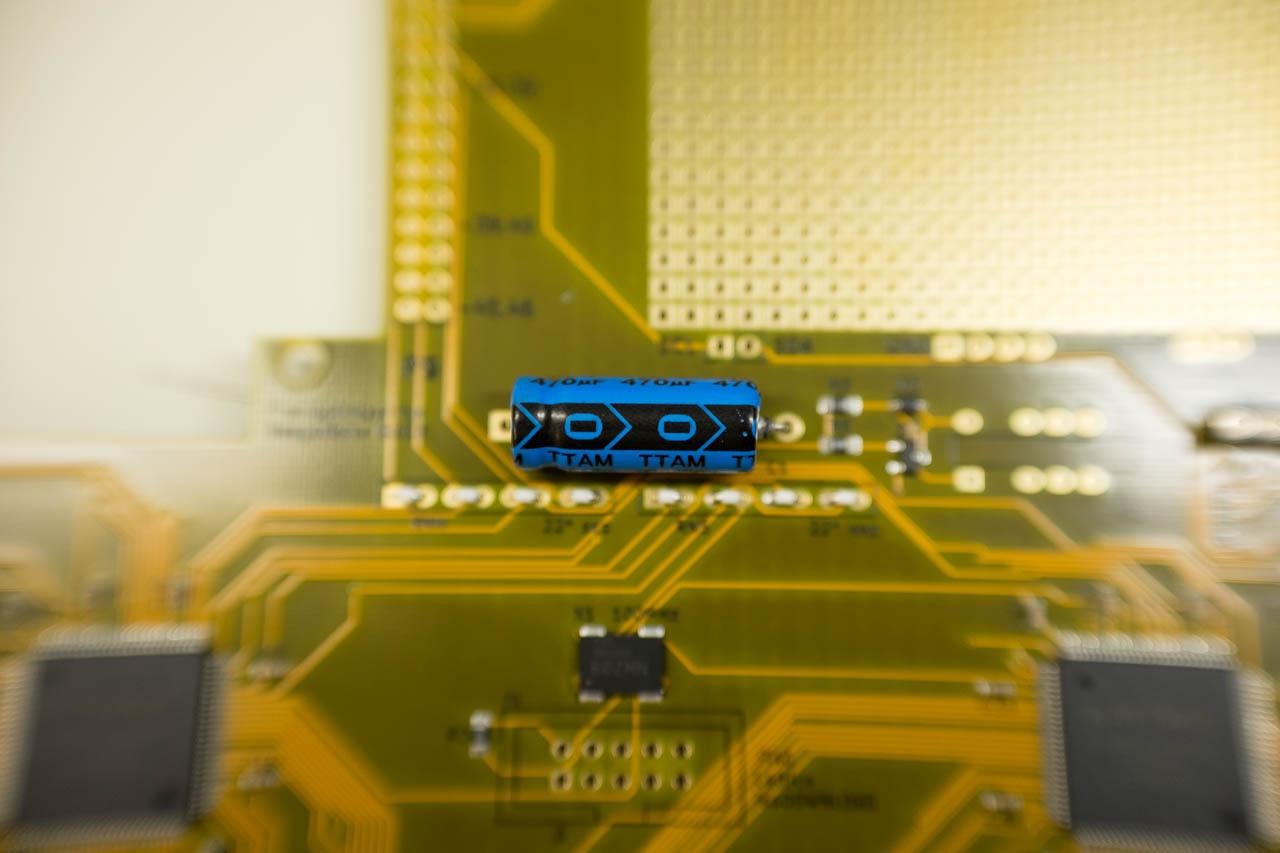
Bend the leads on all 5 capacitors at a right angle, as close to the body of the capacitor as practical.
Note that there is an arrow indicating the NEGATIVE terminal. The PC board has a + indication on the POSITIVE terminal. The capacitors should be installed with the negative arrow pointing away from the + pad on the board. The outline of the part should match the shape on the board.
Insert the large 470uF capacitor into C1.
Insert the other 4 10uF capacitors into C2, C3, C4 and C5.
Ensure the capacitors are sitting all the way down on the board. Push the leads in the holes, push the part onto the board, and then bend the leads on the bottom outwards to a 45 degree angle (roughly!) This is called 'cinching the leads' and keeps the part from falling out!
From the bottom of the board, solder, applying heat to the pad for about half a second first, then applying enough solder to make a small puddle that looks like a tiny pyramid. Enough solder should flow in the hole such that on the top (component) side, a small mount is visible on the top pad as well.
Cut the leads flush with the top of the solder joint with your diagonal or flush cutters.
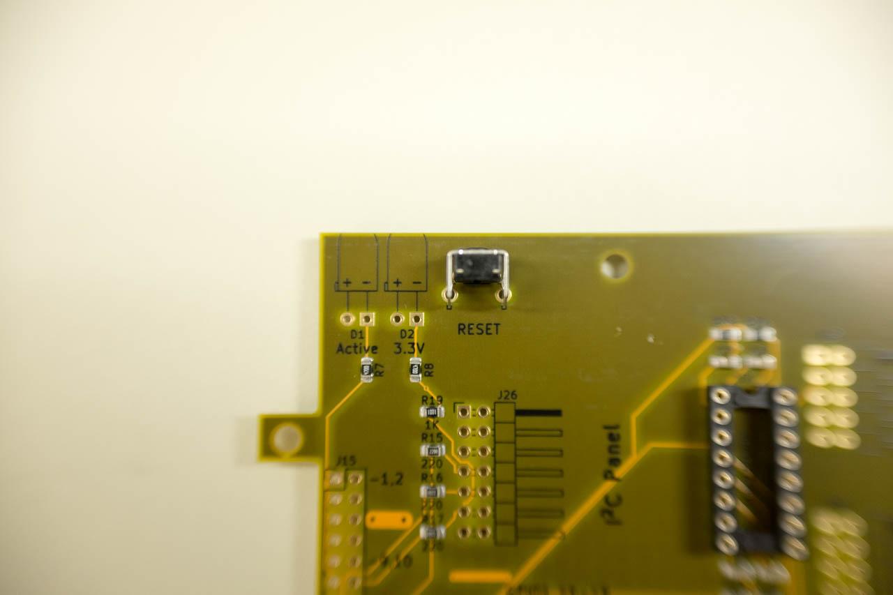
Install the Reset button (short shaft) and the User button (long shaft) at the top of the board and solder.
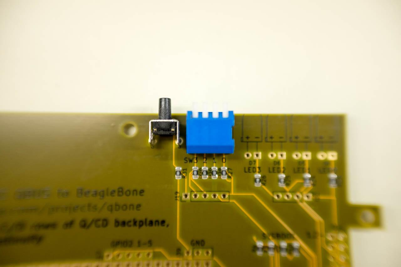
Install the "piano" DIP switch into the top of the board and solder two opposite corner pins, ensuring that the part is flush with the board. Then, solder the remaining pins.
Install the 6-wire terminal block at J8. The openings for wires should point up towards the breadboarding area. Solder to the PCB.
Install the relay at K1 and solder to the board. Be careful, this part has an uneven bottom and it is easy to install (wrongly) at an angle.
Wash the board again under warm water. Scrub gently and dry.


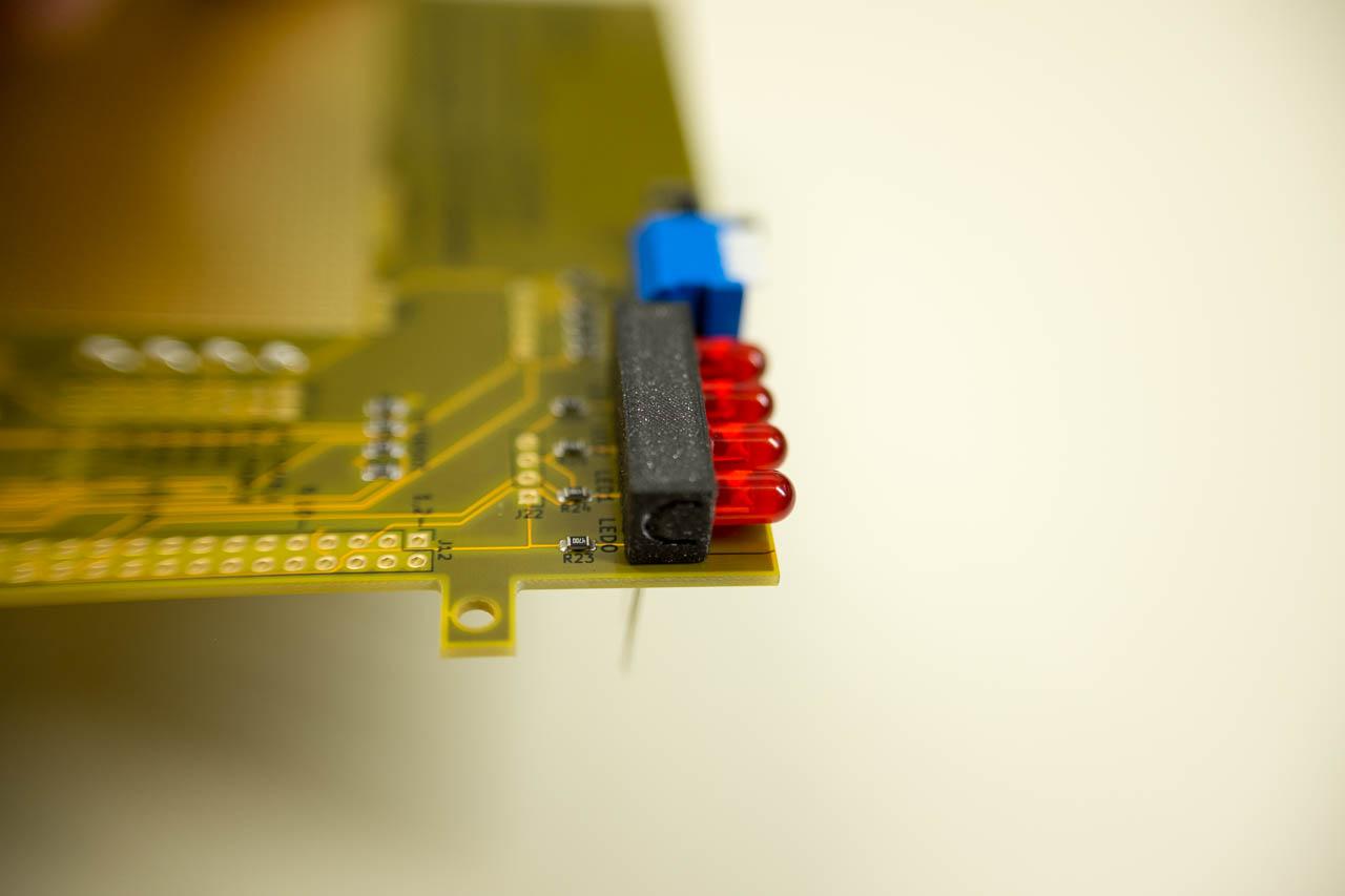
Part 4: LEDs and On-board Headers
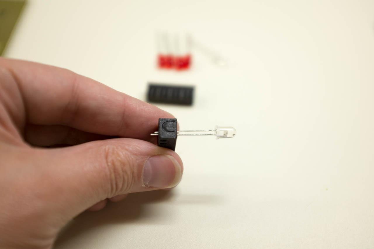
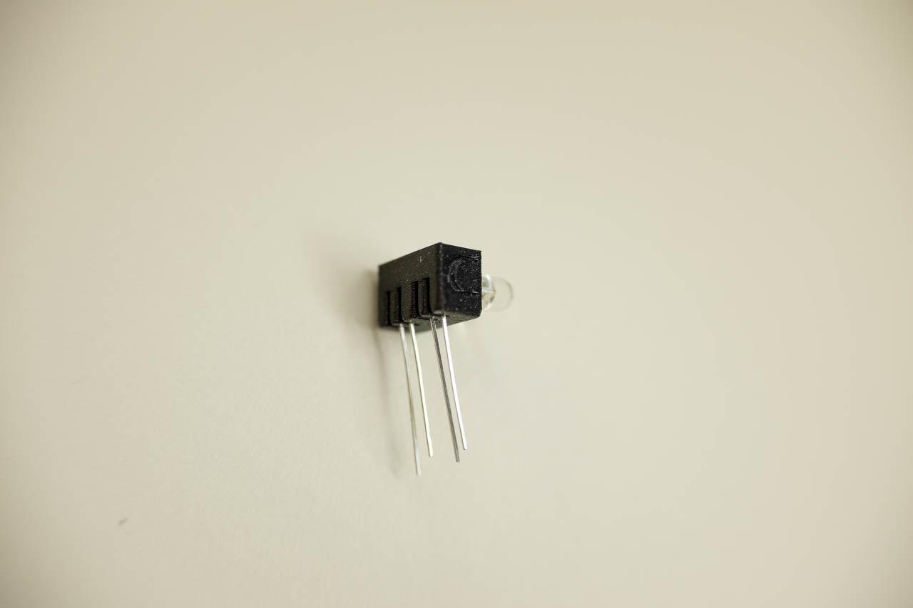
Locate the 2 3D-printed LED holders, the 4 red LEDs, and the 2 green LEDs.
Insert the 4 red LEDs into the larger LED holder. The shorter lead (on the same side of the LED that has a flat spot at its widest point) should be nearest to the side of the holder that has a C printed on it.
Bend the leads down, pushing them into the slots in the holder, so they bend at a right angle.
Insert the 2 green LEDs into the smaller LED holder, using the same approach.
Solder the 4 LEDs in their holder to the PC Board at locations LED1-LED4. Solder a single pin, then ensure the body is straight before contining.
Solder the 2 LEDs in their holder to the PC board at locations "Active" and "3.3V". Be sure to keep the holder square and flat against the board.
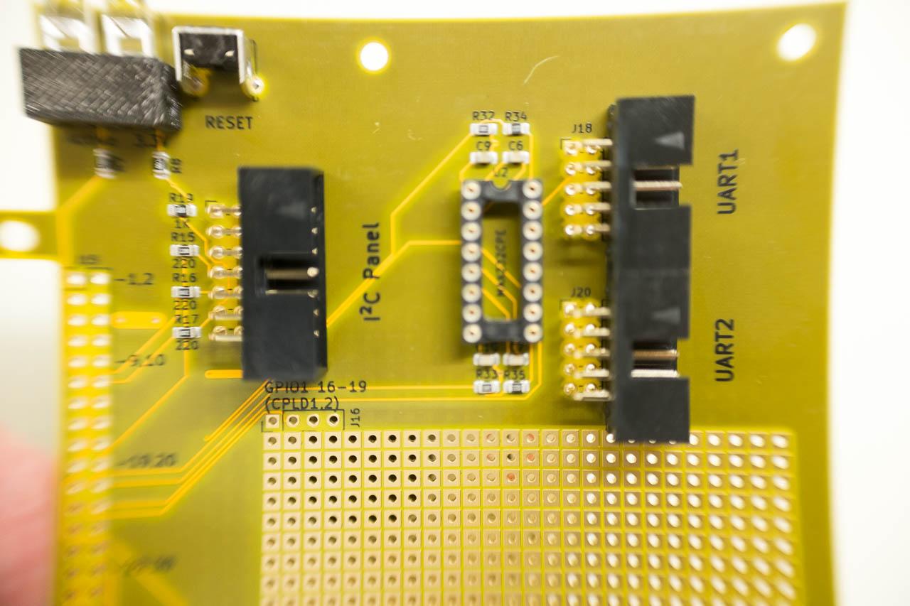
Install the 2 10-pin UART headers (J18 and J20) and solder.
Install the 14-pin I²C Panel header (J26) and solder.
-
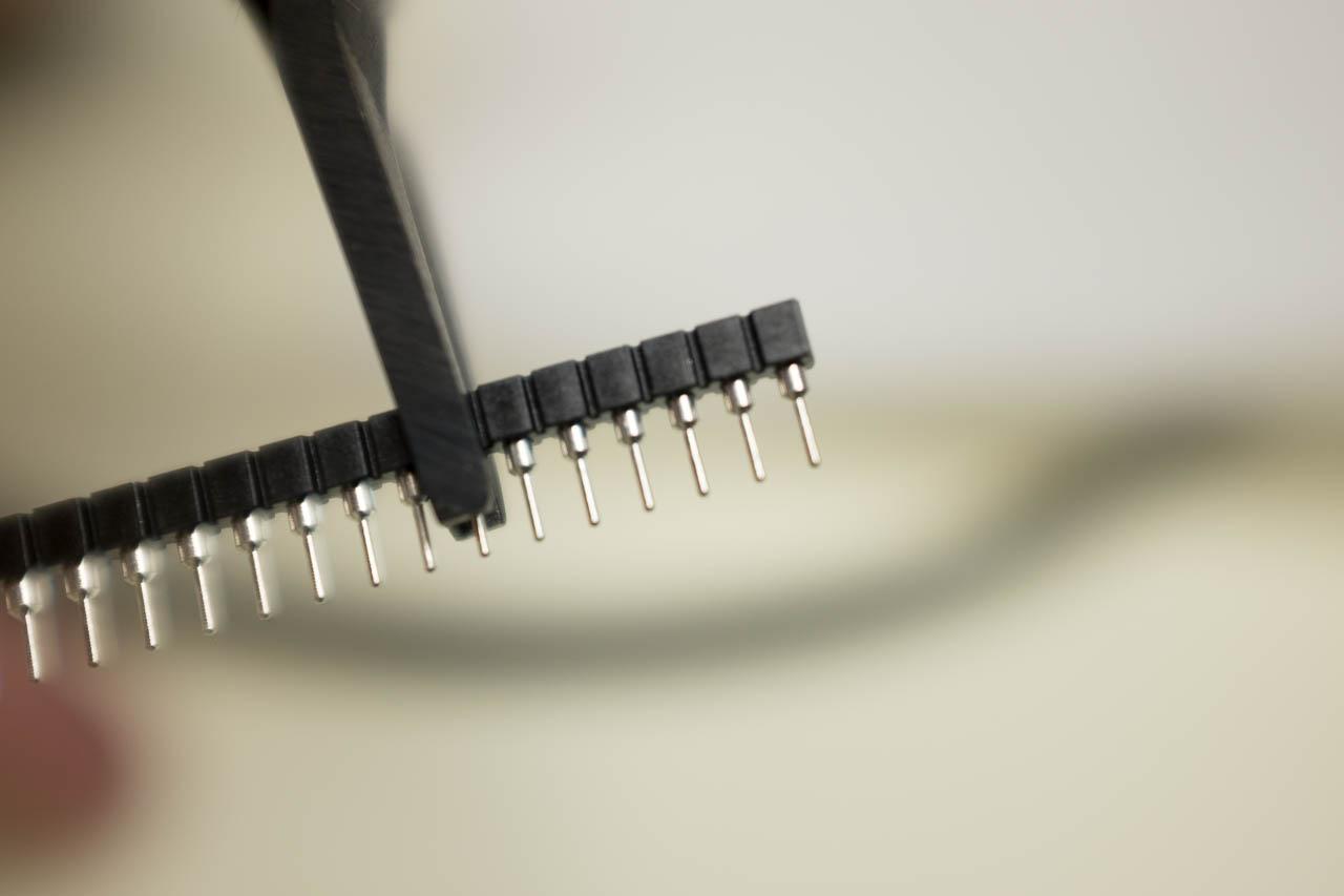
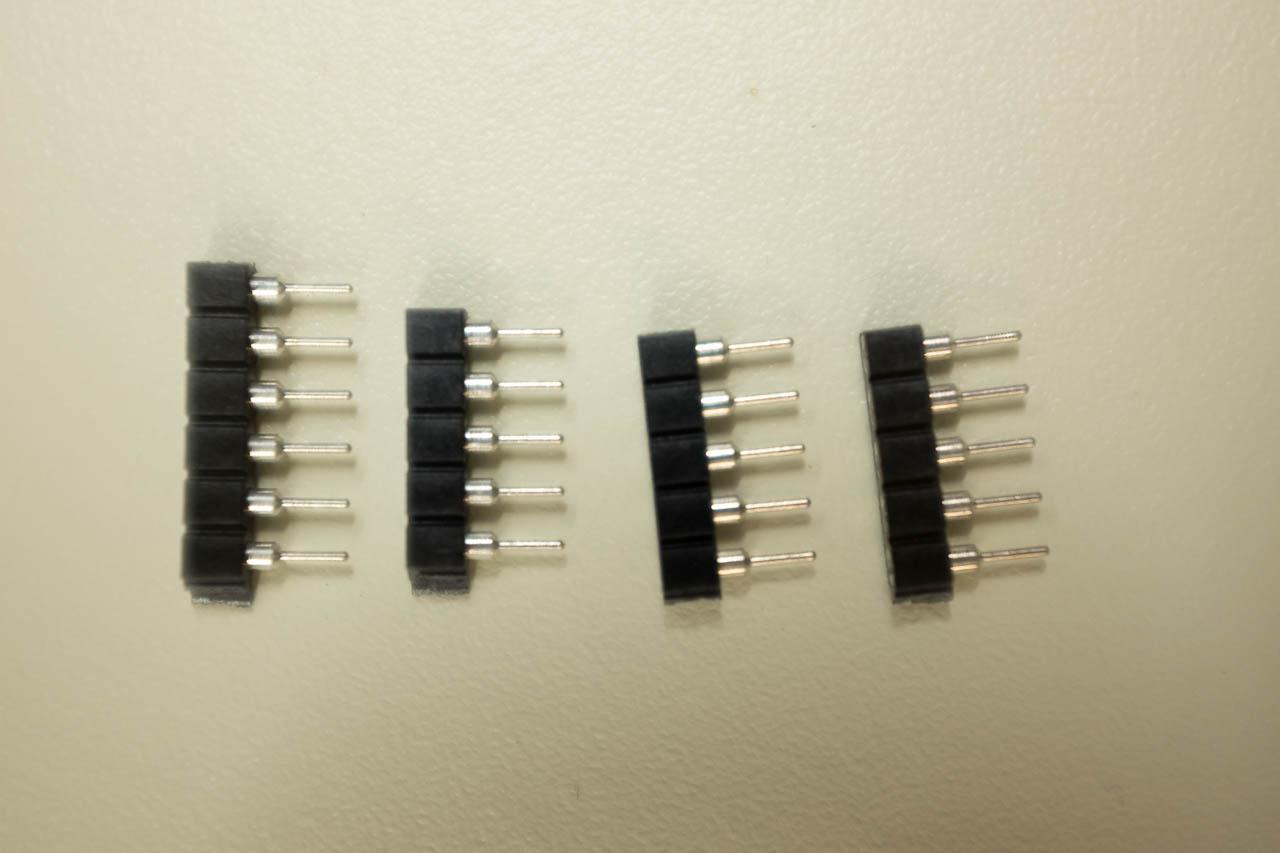
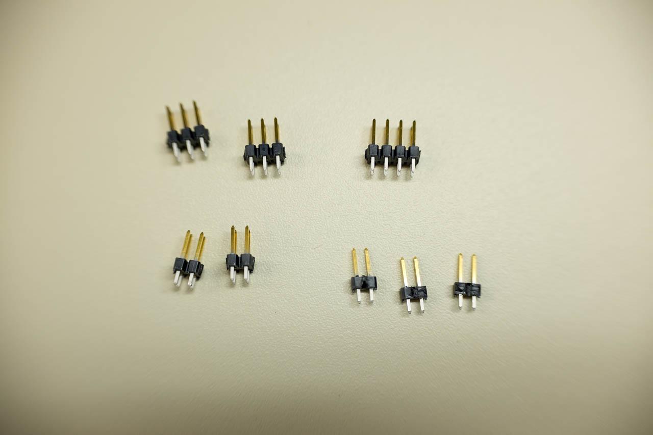
Separate the normal gold-plated headers (these have metal sticking out of both sides of the plastic carrier) into the following sizes. Hold the strip with a pair of pliers, then twist the length you want off using your dominant hand. You need these lengths:
2x 2x3 pins (BDMGI/O, BIAKI/O)
1x 2x2 pins (JP5/JP6)
1x 2x4 pins (Q22)
3x 2x1 pins (JP7, JP8, JP9)
Install a shunt jumper on the gold side of the header, and use this to hold the pins while soldering. A piece of painters' or masking tape may also help. Solder each header to the board, then remove the shunt jumper. You don't want to get the insides of the shunt jumpers wet.
Wash the board yet again under warm water. Scrub gently, and dry.
The next step is the hardest, so take a tea break! You are about 60% done.

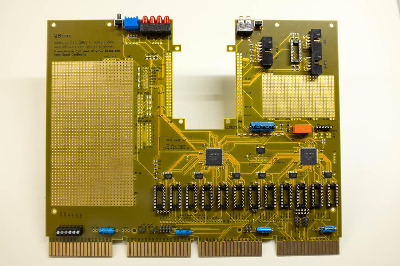
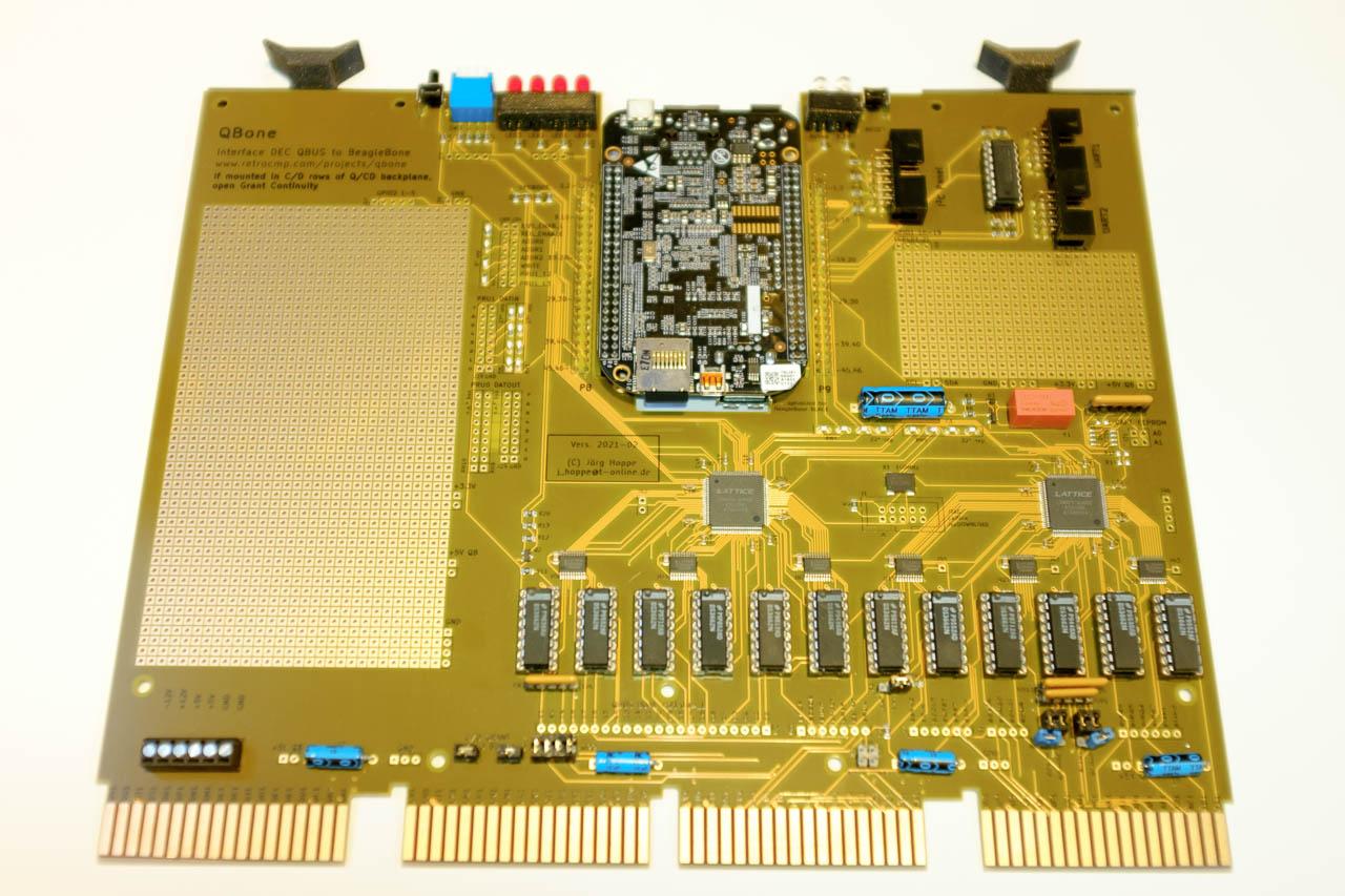
Part 5: Beaglebone interposer boards
If any of this seems confusing, here's our video of this part of the assembly process.
Locate the 2 2x23 headers that have been shifted to one end, with the plastic carrier on the gold side and the pins sticking out on the tinned side.
Insert the header through the provided 3.5mm-thick 3D-printed plastic spacer.
Insert the header/spacer stack through an interposer PCB. It doesn't matter which side you use, or which side is on top, it is symmetrical. Approximately 3mm of tinned pin should be sticking up from the PCB.
Solder the PCB in place, taking extra care to keep the PCB-spacer-header sandwich together with no gaps.
Flip the sandwich over. Using a strong screwdriver, awl, or soldering tool, pry the black plastic carrier off of the pins. Then, remove the 3.5mm spacer.
Trim the solder-side remaining pin length as short as possible, without damaging the soldering joint.
Repeat the above steps for the other interposer PCB.
Wash the interposer boards under warm water. Scrub both sides gently, and pat dry.
While the boards dry, continue:
Separate the tin-plated headers into 2x23 pins. These headers are all tinned, with no gold whatsoever.
Insert the header into the QBone cape, with the black plastic carrier on the bottom of the board (solder side). The pins should be sticking out on the component side.
Tack two corner pins and at least one central pin, ensuring the pin header remains flush with the board at all times. Then, solder all the remaining pins. All of this soldering is on the component side, not the solder side.
Flip the board over. Using a strong screwdriver, awl, or soldering tool, pry the black plastic carrier off of the pins.
Wash the board under warm water. Scrub gently, and dry.
Once all boards are dry (about 20-30 minutes), finish:
If you don't have it on already, put on your anti-static wristband for all assembly steps from here on out.
Install one of the interposer boards into the BeagleBone, with the unsoldered "wing" sticking out from the unit, not inwards.
Place the BeagleBone and its "wing" over the exposed pin stubs of the header you just soldered. The BeagleBone will be upside-down, with its bottom facing up towards the component side of the QBone.
Install the other interposer board into the BeagleBone, placing that "wing" over the remaining QBone pin stubs.
Solder the interposer boards to the QBone cape, ensuring that they stay flush to the QBone on all sides.
Trim the solder-side pin length as short as possible, without damaging the soldering joint.
Remove the BeagleBone, then wash the QBone+interposer boards under warm water. Scrub gently, especially in the pin headers on both sides. Pat dry.
You're done with soldering! Have another tea break. You are 90% done!
Part 6: Final Assembly
-
Install the SIP resistor packs as follows. The text on all packs faces the gold finger edge connectors:
RN6: 10k bus (6X-1-103LF)
RN7: 10k (5X-1-103LF)
RN11: 330 (6x-1-331LF: one pin hangs outside of the SIP header to the RIGHT)
RN12: 680 (5X-1-681LF)
Install the MAX232CPE chip at U2, noting that the pin 1 marking on the IC should be at the top of the socket, away from the gold edge fingers.
Install the 12x driver chips at the edge of the board nearest to the gold fingers. The pin 1 markings on the ICs should be at the top of the socket, away from the gold edge fingers.
-
Install the shunt jumpers as follows:
One jumper each on the C/D Grant 2-pin jumpers, unless the board is going into a backplane with C/D signals.
4 jumpers on the Q22 header, unless the QBone is going in an LSI-11/03 system or equivalent
Place one jumper on a single pin of the EVNT 50Hz jumper, unless you know you need the QBone to generate an LTC. More information.
IRQ/DMA GRANT jumpers are backplane dependent. The loopback jumpers at the bottom should be installed for testing. In most backplanes, place 2 jumpers vertically on each block, and the loopback jumper horizontally at the bottom. More information.
The QBone no longer populates the EEPROM and EEPROM ADDR jumpers as this functionality is not used. So, no jumpers there.
You're done! Have a piece of candy.
You may now proceed to testing, keeping in mind your CPLDs have already been programmed, your microSD card is pre-programmed, and no EEPROM programming is necessary.